


Stephen Shankland | CNET.Com
Troy Warren for CNT #Technology

The chipmaker’s come-from-behind strategy is risky and will take years, even with government subsidies.
I am sweltering inside an Intel chip factory outside Phoenix, bundled head-to-toe in a Gore-Tex suit to keep me from contaminating billions of dollars’ worth of the world’s most delicate fabrication equipment. As plastic pods of silicon wafers whiz from station to station along roof-mounted transit lines, there’s nothing about the room that feels outdated. Still, I think to myself: I’m looking at either the past or the future of American manufacturing.
That’s because Intel is at a fork in the road. One direction leads to a comfortable stasis as a processor designer, perhaps with a side business making chips with yesterday’s technology.
After squandering its lead because of a half decade of problems modernizing its manufacturing, that’s where Intel has been headed. The Silicon Valley icon ceded processor market share to longtime rival AMD, lost the Mac business to Apple’s in-house M-series chips, and fell behind Taiwan Semiconductor Manufacturing Co. (TSMC) and Samsung in making chips.
Pat Gelsinger, Intel’s new chief executive, wants to take the other course: restore the company’s status as the leader of the semiconductor industry, an enormously profitable innovator fueling each year’s advances in phones, PCs, smartwatches, internet services and everything else in our digital lives. Getting there requires a series of major manufacturing upgrades and delivery of a quartet of new chips those upgrades will enable: Alder Lake for gaming PCs this year and laptops next year, Ponte Vecchio and Sapphire Rapids for servers in 2022, and Meteor Lake for PCs in 2023. Intel will have to get everything right after years of getting much of it wrong.
With “a decade of bad decisions, this doesn’t get fixed overnight,” Gelsinger says in an interview. “But the bottom is behind us and the slope is starting to feel increasingly strong.”
Intel’s choice, to coast or to rebuild, is emblematic of one that the entire United States faces. Most of the country’s 20th century manufacturing leadership has migrated to Asia, particularly to China.
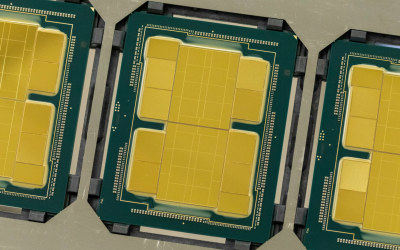
Intel is among the most prominent examples of a company trying to keep US manufacturing vibrant. As I walk through its chip fabrication plants — “fabs” — Gelsinger’s plans are underway. In the CH4 fab, employees wheel around carts packed with Ponte Vecchio processors, assembled from dozens of smaller “chiplets” and likely destined for the Energy Department’s 2022 supercomputer, Aurora. Although Meteor Lake won’t arrive for more than a year, Intel is making dummy versions to debug new chip packaging technology.
More fabs are on the way, too. In an enormous empty patch of dirt at its existing Arizona site, Intel has just begun building fabs 52 and 62 at a total cost of $20 billion, set to make Intel’s most advanced chips, starting in 2024. Later this year, it hopes to announce the US location for its third major manufacturing complex, a 1,000-acre site costing about $100 billion. The spending commitment makes this year’s $3.5 billion upgrade to its New Mexico fab look cheap.
The goal is to restore the US share of chip manufacturing, which has slid from 37% in 1990 to 12% today. “Over the decade in front of us, we should be striving to bring the US to 30% of worldwide semiconductor manufacturing,” Gelsinger says.
Gelsinger has the ear of politicians, including folks in the Biden administration and the US Senate, which in June approved a bill to lavish $52 billion on US semiconductor companies that want to keep essential manufacturing in the US. On Wednesday, House Speaker Nancy Pelosi announced an effort to push the legislation forward through both houses of Congress. If passed into law, it could knock about $3 billion off the $10 billion price tag for each new fab, a subsidy level Gelsinger says would match those of Taiwan and Korea.
But returning Intel to its glory days — and anchoring a resurgent US electronics business in the process — is much easier said than done.
Making chips profitably means running fabs at maximum capacity to pay off the gargantuan investments required to stay at the leading edge. A company that can’t keep pace gets squeezed out, like IBM in 2014 or Global Foundries in 2018. To catch up after its delays, Intel now plans to upgrade its manufacturing five times in the next four years, a breakneck pace by industry standards.
“This new roadmap that they announced is really aggressive,” says Linley Group analyst Linley Gwennap. “I don’t have any idea how they are going to accomplish all of that.”
The return of Pat Gelsinger
Gelsinger grew up on a Pennsylvania farm and joined Intel as a teenager in 1979 as a quality control technician, earning his bachelor’s degree in electrical engineering while at the company. He spent the next three decades at Intel, rising to chip engineer, then leader of the 486 design, then chief technology officer in 2001.
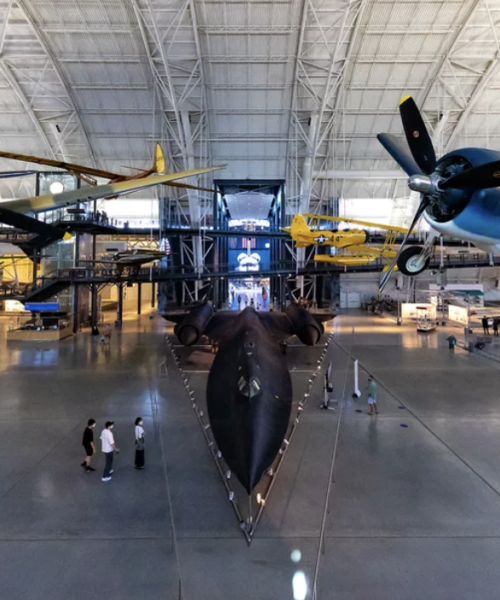
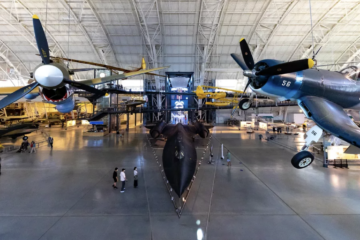
A look inside Intel’s mammoth Arizona chipmaking fab

When it became apparent he wouldn’t be named CEO, Gelsinger quit Intel for storage system maker EMC in 2009, and in 2012 took over its software spinoff, VMware. His dream to lead Intel was realized this February when the board appointed him to replace Bob Swan, Intel’s former chief financial officer, who’d had the job for two years.
Intel’s board endorsed Gelsigner’s plan to steer the company more in the style of the company’s first three technically expert CEOs: co-founder Robert Noyce, Gordon Moore of Moore’s Law fame, and Andy Grove, author of the seminal Silicon Valley business book Only the Paranoid Survive. (Swan didn’t have an engineering background.) Gelsinger aspires to rekindle Grove’s management style, with unflinching assessments and data-backed judgments.
“It was an inspired choice,” says Andrew Feldman, CEO of Cerebras, a startup that designs artificial intelligence chips for its own AI computer systems. As with Microsoft naming Satya Nadella leader, it was time for a “thoughtful technologist.”
Now Gelsinger has a tech-first recovery plan. He’s pledged to accelerate manufacturing upgrades to match the technology of TSMC and Samsung by 2024 and surpass them in 2025. He’s opening Intel’s fabs to other companies that need chips built through its new Intel Foundry Services (IFS). And he’s relying on other foundries, including TSMC, for about a quarter of Intel’s near-term chipmaking needs to keep its chips more competitive during the upgrades.
This three-pronged strategy is called IDM (integrated design and manufacturing) 2.0. That’s a new take on Intel’s philosophy of both designing and making chips. It’s more ambitious than the future some had expected, in which Intel would sell its factories and join the ranks of “fabless” chip designers like Nvidia, AMD and Qualcomm that rely on others for manufacturing.
The cost of Intel’s recovery
Gelsinger secured full support of Intel’s board of directors before setting off on the plan.
“As I was interviewing for the job, I wrote a strategy paper for the board,” Gelsigner says. “I demanded unity so every one of them had to say they were hiring me and agreeing with the strategy.”
It’s a good thing he did. In October, investor enthusiasm for Gelsinger’s return soured when Intel revealed IDM 2.0’s costs in its third-quarter financial results. Intel expects to generate $2 billion in cash in 2022, down from $20 billion in 2020, as capital expenditures on new fabs soars to $25 billion to $28 billion and profit margins plunge. Intel shares dropped 12% after the October announcement.
INTEL’S TOUGH ROAD TO RECOVERY
Intel will outpace Moore’s Law, CEO Pat Gelsinger says
Apple’s M1 Pro and M1 Max chips mean new trouble for Intel
Qualcomm, Amazon boost Intel plan to leapfrog chipmaking rivals by 2025
Intel will make others’ chips in major turnaround effort under new CEO
Stacy Rasgon, an analyst at Bernstein Research, lowered his target for Intel shares from $43 to $40, expressing concern about “ballooning” expenses and worrying that Intel is counting on PC market growth that won’t actually happen. Intel’s expectation that revenue will grow 10% to 12% annually for the next four to five years “seems outlandish,” he said in a research note.
Shareholders may not like Gelsinger’s spending-heavy strategy, but one community really does: Intel’s engineers.
“It’s really something when your CEO gets excited about new technology. The first question he asks you is ‘How soon can I get it?’ versus ‘I don’t have money to invest here,'” says Babak Sabi, who leads Intel’s assembly and test development work. “If you look at the technical community, we’re jazzed up. We love it. Pat has been really the best thing that has happened.”
Gelsigner has doubled the number of silicon wafers that Intel’s Technology Development (TD) team gets to send through Intel’s fabs to test and debug new technology. That work is costly because the development wafers take the place of revenue-generating wafers for chip production. But Gelsinger judges it necessary to find and fix problems with next-gen manufacturing. With over 500 processing steps required, it takes three months or more to make a single chip, so each wafer is precious.
Gelsigner told the board that Intel is done with stock buybacks, a financial move in which a company uses its cash to buy stock and thereby increase its price. “We’re investing in factories,” he told me. “That’s going to be the use of our cash.”

This empty dirt lot in Chandler, Arizona, is where Intel has begun building Fab 52 and Fab 62, a pair of chip factories costing $10 billion each that should go online in 2024. This photo is from the roof of Fab 42.
Necessary steps to fix Intel’s manufacturing
Historically, progress in processor manufacturing has been charted by Moore’s Law. For decades, miniaturization meant chipmakers could, every two years, double a chip’s tally of tiny on-off switches, called transistors.
Chipmaking processes traditionally have been measured in circuitry feature sizes that stretch just nanometers, or billionths of a meter. A human hair is about 100,000 nanometers wide. Intel’s current problems stemmed from its difficulties moving from its 14-nanometer process to its 10nm process.
But the nanometer label has become merely ornamental as miniaturization progress has slowed. Chipmakers now often focus on improving not just the area each transistor occupies but also its performance and power consumption, together called PPA.
Under Gelsinger, Intel renamed its manufacturing process nodes, part of an effort to align its steps with those of Samsung and TSMC. What had been called 10nm Enhanced Superfin became Intel 7. That’s the process used to build the Alder Lake PC processors, formally called 12th Gen Core, that just started shipping.
That’s just the first milestone Intel has committed to. Intel’s chip manufacturing road map then promises annual improvements:
• Intel 4, with a 20% performance boost over Intel 7. Intel will use it for the Meteor Lake PC chip starting in 2022 and shipping in 2023. Intel 4 will be the first Intel node to adopt a manufacturing technique that TSMC and Samsung already use, extreme ultraviolet (EUV) light, for smaller transistors.
• Intel 3 should arrive in late 2023, a refinement offering an 18% speed boost over Intel 4.
• Intel 20A in 2024 is a radical overhaul. Its core developments are “RibbonFET,” Intel’s name for the gate-all-around transistor structure upgrade, and “PowerVia,” its plan for delivering electrical power through the back of the chip.
• Intel 18A in 2025 is a faster refinement, though Intel hasn’t detailed the expected performance improvement.
The A signals Intel’s “angstrom era” labels; 1 angstrom is about the diameter of a hydrogen atom, and 10 angstroms equals 1 nanometer.
“We cannot recall the last time Intel put so many stakes in the ground,” said BMO Capital Markets analyst Ambrish Srivastava in a July research report after Intel announced its schedule.


In Other NEWS